


| CPU | Arm Cortex-R4F |
| Frequency (MHz) | 180, 120 |
| ADC | 2 x 12-Bit (24ch), 2 x 12-Bit (16ch) |
| GPIO | 64, 45 |
| UART | 1, 2 |
| Number of I2Cs | 1 |
| Features | Hercules high-performance microcontroller |
| TI functional safety category | Functional Safety-Compliant |
| Operating temperature range (C) | -40 to 105 |
- High-Performance Microcontroller (MCU) for Safety-Critical Applications
- Dual CPUs Running in Lockstep
- ECC on Flash and RAM Interfaces
- Built-In Self-Test (BIST) for CPU and On-chip RAMs
- Error Signaling Module With Error Pin
- Voltage and Clock Monitoring
- ARM Cortex-R4F 32-Bit RISC CPU
- 1.66 DMIPS/MHz With 8-Stage Pipeline
- FPU With Single and Double Precision
- 12-Region Memory Protection Unit (MPU)
- Open Architecture With Third-Party Support
- Operating Conditions
- Up to 180-MHz System Clock
- Core Supply Voltage (VCC): 1.14 to 1.32 V
- I/O Supply Voltage (VCCIO): 3.0 to 3.6 V
- Integrated Memory
- Up to 1MB of Flash With ECC
- 128KB of RAM With ECC
- 64KB of Flash for Emulated EEPROM With ECC
- Common Platform Architecture
- Consistent Memory Map Across Family
- Real-Time Interrupt Timer (RTI) OS Timer
- 128-Channel Vectored Interrupt Module (VIM)
- 2-Channel Cyclic Redundancy Checker (CRC)
- Direct Memory Access (DMA) Controller
- 16 Channels and 32 Peripheral Requests
- Parity for Control Packet RAM
- DMA Accesses Protected by Dedicated MPU
- Frequency-Modulated Phase-Locked Loop (FMPLL) With Built-In Slip Detector
- IEEE 1149.1 JTAG, Boundary Scan and ARM CoreSight Components
- Advanced JTAG Security Module (AJSM)
- Up to 64 General-Purpose I/O (GIO) Pins
- Up to 16 GIO Pins With Interrupt Generation Capability
- Enhanced Timing Peripherals
- 7 Enhanced Pulse Width Modulator (ePWM) Modules
- 6 Enhanced Capture (eCAP) Modules
- 2 Enhanced Quadrature Encoder Pulse (eQEP) Modules
- Two Next Generation High-End Timer (N2HET) Modules
- N2HET1: 32 Programmable Channels
- N2HET2: 18 Programmable Channels
- 160-Word Instruction RAM With Parity Protection Each
- Each N2HET Includes Hardware Angle Generator
- Dedicated High-End Timer Transfer Unit (HTU) for Each N2HET
- Two 12-Bit Multibuffered ADC Modules
- ADC1: 24 Channels
- ADC2: 16 Channels
- 16 Shared Channels
- 64 Result Buffers With Parity Protection Each
- Multiple Communication Interfaces
- Up to Three CAN Controllers (DCANs)
- 64 Mailboxes With Parity Protection Each
- Compliant to CAN Protocol Version 2.0A and 2.0B
- Inter-Integrated Circuit (I2C)
- 3 Multibuffered Serial Peripheral Interfaces (MibSPIs)
- 128 Words With Parity Protection Each
- 8 Transfer Groups
- One Standard Serial Peripheral Interface (SPI) Module
- Two UART (SCI) Interfaces, One With Local Interconnect Network (LIN 2.1) Interface Support
- Up to Three CAN Controllers (DCANs)
- Packages
- 144-Pin Quad Flatpack (PGE) [Green]
- 100-Pin Quad Flatpack (PZ) [Green]
All trademarks are the property of their respective owners.
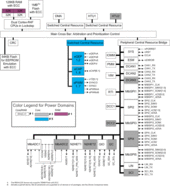
The RM44Lx20 device is part of the Hercules RM series of high-performance industrial-grade ARM? Cortex?-R-based MCUs. Comprehensive documentation, tools, and software are available to assist in the development of IEC61508 functional safety applications. Start evaluating today with the Hercules RM LaunchPad Development Kit. The RM44Lx20 device has on-chip diagnostic features including: dual CPUs in lockstep; CPU and memory Built-In Self-Test (BIST) logic; ECC on both the flash and the SRAM; parity on peripheral memories; and loopback capability on most peripheral I/Os.
The RM44Lx20 device integrates the ARM Cortex-R4F floating-point CPU which offers an efficient 1.66 DMIPS/MHz, and has configurations which can run up to 180 MHz providing up to 298 DMIPS. The RM44Lx20 device supports the little-endian [LE] format.
The RM44Lx20 device has up to 1MB of integrated flash and 128KB of RAM configurations with single-bit error correction and double-bit error detection. The flash memory on this device is nonvolatile, electrically erasable and programmable, and is implemented with a 64-bit-wide data bus interface. The flash operates on a 3.3-V supply input (same level as the I/O supply) for all read, program, and erase operations. The SRAM supports single-cycle read and write accesses in byte, halfword, word, and doubleword modes throughout the supported frequency range.
The RM44Lx20 device features peripherals for real-time control-based applications, including two Next-Generation High-End Timer (N2HET) timing coprocessors with up to 44 total I/O terminals, seven Enhanced PWM (ePWM) modules with up to 14 outputs, six Enhanced Capture (eCAP) modules, two Enhanced Quadrature Encoder Pulse (eQEP) modules, and two 12-bit Analog-to-Digital Converters (ADCs) supporting up to 24 inputs.
The N2HET is an advanced intelligent timer that provides sophisticated timing functions for real-time applications. The timer is software-controlled, using a reduced instruction set, with a specialized timer micromachine and an attached I/O port. The N2HET can be used for pulse-width-modulated outputs, capture or compare inputs, or general-purpose I/O (GIO). The N2HET is especially well suited for applications requiring multiple sensor information and drive actuators with complex and accurate time pulses. A High-End Timer Transfer Unit (HTU) can transfer N2HET data to or from main memory. A Memory Protection Unit (MPU) is built into the HTU.
The ePWM module can generate complex pulse width waveforms with minimal CPU overhead or intervention. The ePWM is easy to use and supports complementary PWMs and deadband generation. With integrated trip zone protection and synchronization with the on-chip MibADC, the ePWM is ideal for digital motor control applications.
The eCAP module is essential in systems where the accurately timed capture of external events is important. The eCAP can also be used to monitor the ePWM outputs or to generate simple PWM when not needed for capture applications.
The eQEP module is used for direct interface with a linear or rotary incremental encoder to get position, direction, and speed information from a rotating machine as used in high-performance motion and position-control systems.
The device has two 12-bit-resolution MibADCs with 24 total inputs and 64 words of parity-protected buffer RAM each. The MibADC channels can be converted individually or can be grouped by software for sequential conversion sequences. Sixteen inputs are shared between the two MibADCs. There are three separate groups. Each group can be converted once when triggered or configured for continuous conversion mode. The MibADC has a 10-bit mode for use when compatibility with older devices or faster conversion time is desired.
The device has multiple communication interfaces: three MibSPIs; two SPIs; two SCIs, one of which can be used as LIN; up to three DCANs; and one I2C module. The SPI provides a convenient method of serial interaction for high-speed communications between similar shift-register type devices. The LIN supports the Local Interconnect standard 2.0 and can be used as a UART in full-duplex mode using the standard Non-Return-to-Zero (NRZ) format. The DCAN supports the CAN 2.0B protocol standard and uses a serial, multimaster communication protocol that efficiently supports distributed real-time control with robust communication rates of up to 1 Mbps. The DCAN is ideal for applications operating in noisy and harsh environments (for example, automotive and industrial fields) that require reliable serial communication or multiplexed wiring.
The I2C module is a multimaster communication module providing an interface between the microcontroller and an I2C-compatible device through the I2C serial bus. The I2C module supports speeds of 100 and 400 kbps.
A Frequency-Modulated Phase-Locked Loop (FMPLL) clock module is used to multiply the external frequency reference to a higher frequency for internal use. The FMPLL provides one of the six possible clock source inputs to the Global Clock Module (GCM). The GCM manages the mapping between the available clock sources and the device clock domains.
The device also has an external clock prescaler (ECP) circuit that when enabled, outputs a continuous external clock on the ECLK terminal. The ECLK frequency is a user-programmable ratio of the peripheral interface clock (VCLK) frequency. This low-frequency output can be monitored externally as an indicator of the device operating frequency.
The Direct Memory Access (DMA) controller has 16 channels, 32 peripheral requests, and parity protection on its memory. An MPU is built into the DMA to protect memory against erroneous transfers.
The Error Signaling Module (ESM) monitors device errors and determines whether an interrupt or external error signal (nERROR) is asserted when a fault is detected. The nERROR terminal can be monitored externally as an indicator of a fault condition in the microcontroller.
With integrated functional safety features and a wide choice of communication and control peripherals, the RM44Lx20 device is an ideal solution for high-performance, real-time control applications with safety-critical


